Analog and Mixed-Signal Circuit Design Grand Challenges

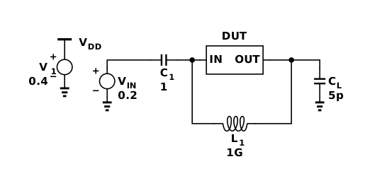
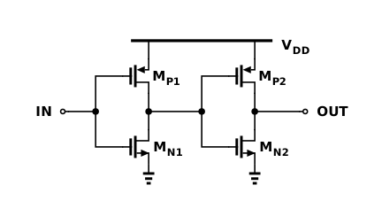
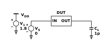
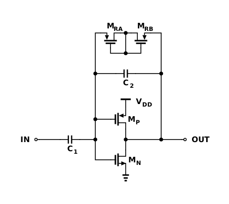
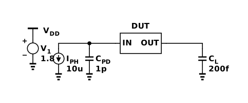
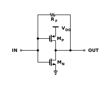
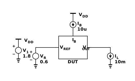
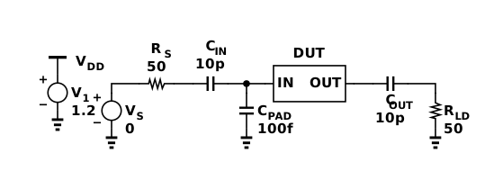
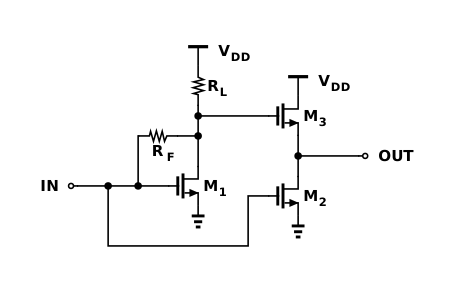
Each challenge is a fixed testbench around a black-box DUT; only the box is designed. Each runnable question is implemented twice, open (SKY130 PDK, ngspice) and closed (GF22 22FDX+ PDK, Cadence Spectre), shown side by side; the design challenges use open PDKs and ngspice. The baseline of each question is the best structure we know for it and scores 0; a score is log10 of the improvement over it. Signal sources drive the DUT through at least 50 Ω.

Runnable questionsopen (SKY130, ngspice) and closed (GF22 22FDX+, Spectre) implementations

Q1Amplifier structure that maximises fu/P

Maximise fu/P, bias current included

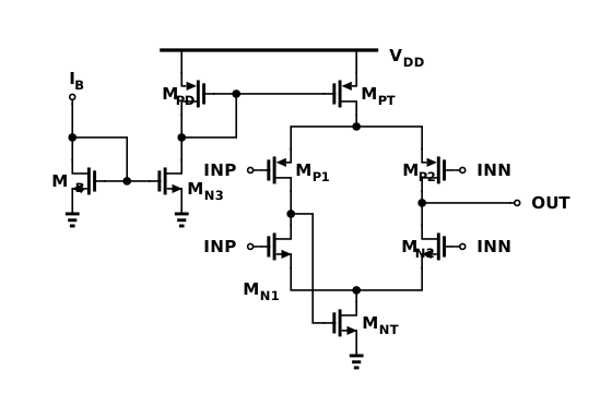
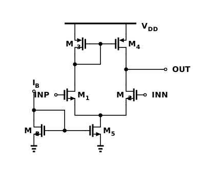
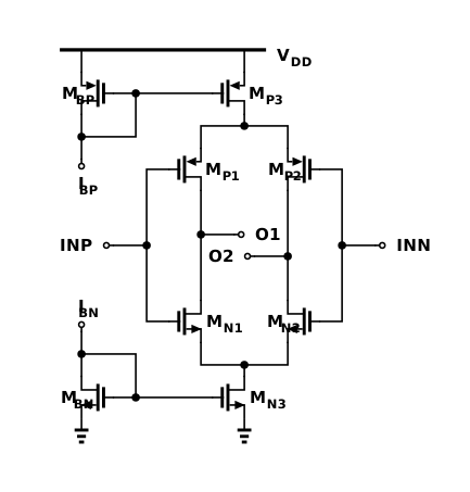
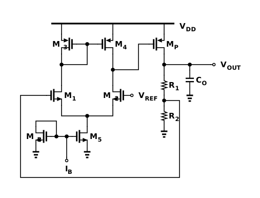
Baseline structure Current-reuse OTA: PMOS and NMOS input pairs stacked on one bias current, PMOS tail mirrored from IB, NMOS tail closing the common-mode loop
OpenSKY130 · ngspice

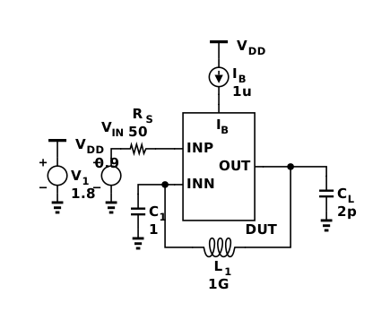
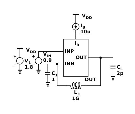
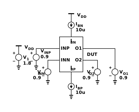
Testbench (SKY130): 1.8 V supply, 1 µA into IB, 0.9 V through 50 Ω on INP, a 1 GH and 1 F loop from OUT to INN, 2 pF loadTestbench.ac .noise · PVTSKY130Baseline: Current-reuse OTA: PMOS and NMOS input pairs stacked on one bias current, PMOS tail mirrored from IB, NMOS tail closing the common-mode loopBaseline

Baseline 1.48 MHz/µW
Power16.7 µW
Gain44.5 dB
fu24.7 MHz
Phase margin70°
Worst PVT41.4 dB, 67°, 15.5 MHz

Gates for any design Gain ≥ 40 dB, PM ≥ 60°, fu ≥ 5 MHz at every PVT corner

Previous baseline five-transistor OTA: 0.378 MHz/µW, score −0.59

ClosedGF22 22FDX+ · Spectre

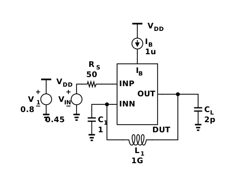
Testbench (GF22 22FDX+): 0.8 V supply, 1 µA into IB, 0.45 V through 50 Ω on INP, a 1 GH and 1 F loop from OUT to INN, 2 pF loadTestbench.ac .noise · PVTGF22 22FDX+Baseline: Current-reuse OTA: PMOS and NMOS input pairs stacked on one bias current, PMOS tail mirrored from IB, NMOS tail closing the common-mode loopBaseline
Baseline 2.53 MHz/µW
Power14.4 µW
Gain50.6 dB
fu36.6 MHz
Phase margin84°
Worst PVT36.6 dB, 83°, 28.4 MHz

Gates for any design Gain ≥ 34 dB, PM ≥ 60°, fu ≥ 5 MHz at every PVT corner

Previous baseline five-transistor OTA: 1.11 MHz/µW, score −0.36
Q2Amplifier structure that minimises vn,rms2·P

Minimise input noise from 1 MHz to πfu/2 × power

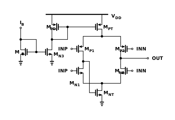
Baseline structure Current-reuse OTA: PMOS and NMOS input pairs stacked on one bias current, PMOS tail mirrored from IB, NMOS tail closing the common-mode loop
OpenSKY130 · ngspice

Testbench (SKY130): 1.8 V supply, 1 µA into IB, 0.9 V through 50 Ω on INP, a 1 GH and 1 F loop from OUT to INN, 2 pF loadTestbench.ac .noise · PVTSKY130Baseline: Current-reuse OTA: PMOS and NMOS input pairs stacked on one bias current, PMOS tail mirrored from IB, NMOS tail closing the common-mode loopBaseline
Baseline 1.01×10⁻¹³ V²W

Input noise78 µV rms
Power16.7 µW
Gain44.5 dB
fu24.7 MHz

Gates for any design Gain ≥ 40 dB, PM ≥ 60°, fu ≥ 5 MHz at every PVT corner

Previous baseline five-transistor OTA: 2.22×10⁻¹³ V²W, score −0.34

ClosedGF22 22FDX+ · Spectre

Testbench (GF22 22FDX+): 0.8 V supply, 1 µA into IB, 0.45 V through 50 Ω on INP, a 1 GH and 1 F loop from OUT to INN, 2 pF loadTestbench.ac .noise · PVTGF22 22FDX+Baseline: Current-reuse OTA: PMOS and NMOS input pairs stacked on one bias current, PMOS tail mirrored from IB, NMOS tail closing the common-mode loopBaseline

Baseline 1.18×10⁻¹⁴ V²W

Input noise38.5 µV rms
Power7.99 µW
Gain53.7 dB
fu18.2 MHz

Gates for any design Gain ≥ 34 dB, PM ≥ 60°, fu ≥ 5 MHz at every PVT corner

Previous baseline five-transistor OTA: 3.05×10⁻¹⁴ V²W, score −0.41

Q3Comparator structure that minimises Tdelay·E/conv

Minimise delay at 1 mV × energy per decision

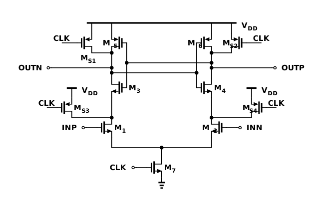
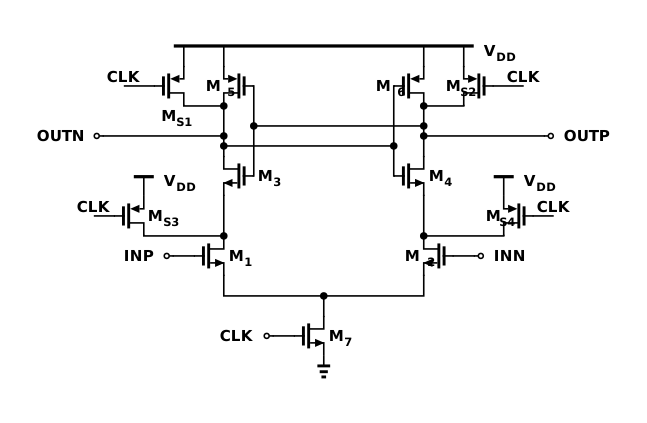
Baseline structure StrongARM latch sized for delay × energy

OpenSKY130 · ngspice

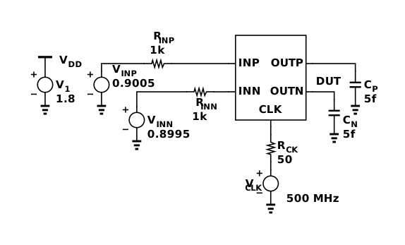
Testbench (SKY130): 1.8 V supply, 500 MHz clock through 50 Ω, inputs 0.9 V ± 0.5 mV through 1 kΩ, 5 fF on each outputTestbench.tran · PVT · MCSKY130Baseline: StrongARM latch sized for delay × energyBaseline

Baseline 2.49×10⁻²³ s·J

Delay at 1 mV315 ps
Energy79 fJ
Input noise612 µV rms
Offset 3σ34.9 mV
Kickback67.9 mV

Gates for any design Resolves, resets to within 50 mV at every PVT corner; offset 3σ ≤ 40 mV; kickback ≤ 100 mV; noise ≤ 1 mV rms

Previous baseline StrongARM latch, first sizing: 3.39×10⁻²³ s·J, score −0.13

ClosedGF22 22FDX+ · Spectre

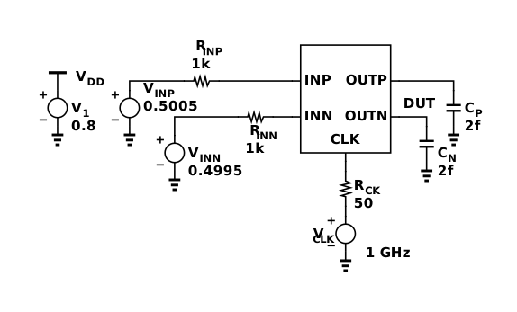
Testbench (GF22 22FDX+): 0.8 V supply, 1 GHz clock through 50 Ω, inputs 0.5 V ± 0.5 mV through 1 kΩ, 2 fF on each outputTestbench.tran · PVT · MCGF22 22FDX+Baseline: StrongARM latch sized for delay × energyBaseline

Baseline 3.87×10⁻²⁵ s·J

Delay at 1 mV53 ps
Energy7.3 fJ
Input noise1.39 mV rms
Offset 3σ23.3 mV
Kickback87.9 mV

Gates for any design Resolves, resets to within 20 mV at every PVT corner; offset 3σ ≤ 30 mV; kickback ≤ 150 mV; noise ≤ 2 mV rms

Previous baseline StrongARM latch, first sizing: 5.73×10⁻²⁵ s·J, score −0.17

Q4Comparator structure that minimises vn,rms2·E/conv

Minimise input-referred noise² × energy per decision (open: LPTV, white + flicker from 10 kHz; closed: Spectre transient noise, 1 MHz to 300 GHz)

Baseline structure StrongARM latch sized for noise × energy (wide input pair)

A floating-inverter-amplifier (FIA) comparator, the published best for this metric, did not beat this StrongARM in our benches: 1.47×10⁻²⁰ against 1.36×10⁻²⁰ V²J (GF22) and 6.8×10⁻²⁰ against 1.50×10⁻²⁰ V²J (SKY130); it is in try/fia.py of each version.

OpenSKY130 · ngspice

Testbench (SKY130): 1.8 V supply, 500 MHz clock through 50 Ω, inputs 0.9 V ± 0.5 mV through 1 kΩ, 5 fF on each outputTestbench.tran + LPTV noise · MCSKY130Baseline: StrongARM latch sized for noise × energy (wide input pair)Baseline

Baseline 1.50×10⁻²⁰ V²J

Delay at 1 mV440 ps
Energy199 fJ
Input noise274 µV rms
Offset 3σ11 mV
Kickback64.4 mV

Gates for any design Resolves, resets to within 50 mV at every PVT corner; offset 3σ ≤ 40 mV; kickback ≤ 100 mV; delay ≤ 500 ps

Previous baseline StrongARM latch, first sizing: 3.79×10⁻²⁰ V²J, score −0.40

ClosedGF22 22FDX+ · Spectre

Testbench (GF22 22FDX+): 0.8 V supply, 1 GHz clock through 50 Ω, inputs 0.5 V ± 0.5 mV through 1 kΩ, 2 fF on each outputTestbench.tran noise · MCGF22 22FDX+Baseline: StrongARM latch sized for noise × energy (wide input pair)Baseline

Baseline 1.36×10⁻²⁰ V²J

Delay at 1 mV53.6 ps
Energy11.2 fJ
Input noise1.1 mV rms
Offset 3σ16.6 mV
Kickback124 mV

Gates for any design Resolves, resets to within 20 mV at every PVT corner; offset 3σ ≤ 30 mV; kickback ≤ 150 mV; delay ≤ 100 ps

Previous baseline StrongARM latch, first sizing: 1.93×10⁻²⁰ V²J, score −0.15

Q5PLL phase detector that minimises trms2·P

Minimise timing noise² (white + flicker, 10 kHz to half the reference rate) × power, VCO-source power included

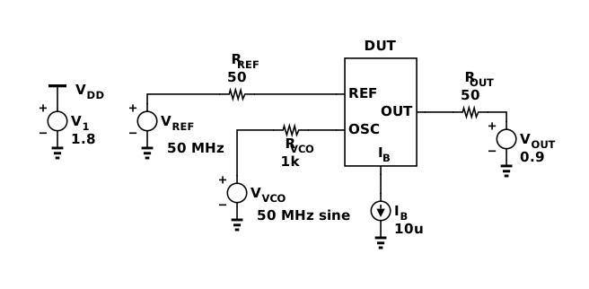
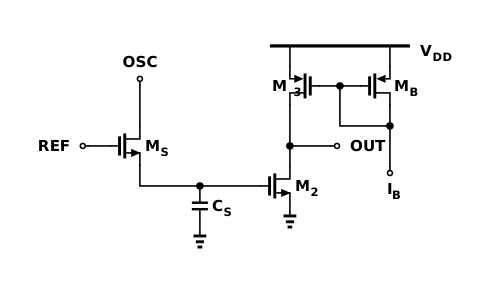
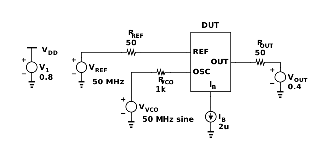
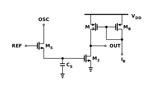
Baseline structure Sampling phase detector: REF samples the VCO sine on OSC onto CS, M2 turns the held voltage into output current

OpenSKY130 · ngspice

Testbench (SKY130): 1.8 V supply, 50 MHz reference through 50 Ω, 50 MHz VCO sine 0.9 ± 0.3 V through 1 kΩ, OUT held at 0.9 V through 50 Ω, 10 µA drawn from IBTestbenchlock + .tran + LPTV · PVTSKY130Baseline: Sampling phase detector: REF samples the VCO sine on OSC onto CS, M2 turns the held voltage into output currentBaseline

Baseline −242.5 dB

Timing noise3.92 ps rms
Power36.4 µW
Gain |∂Q/∂t|72.9 µA
Kickback on VCO45 mV

Gates for any design Locks at every PVT corner; kickback ≤ 50 mV; |∂Q/∂t| ≥ 50 µA (25 µA at every PVT corner); P ≤ 100 µW

Previous baseline sampling PD, first sizing: −240.1 dB, score −0.25

ClosedGF22 22FDX+ · Spectre

Testbench (GF22 22FDX+): 0.8 V supply, 50 MHz reference through 50 Ω, 50 MHz VCO sine 0.4 ± 0.15 V through 1 kΩ, OUT held at 0.4 V through 50 Ω, 2 µA drawn from IBTestbenchPSS + pnoise · PVTGF22 22FDX+Baseline: Sampling phase detector: REF samples the VCO sine on OSC onto CS, M2 turns the held voltage into output currentBaseline

Baseline −248.8 dB

Timing noise5.97 ps rms
Power3.66 µW
Gain |∂Q/∂t|16.4 µA
Kickback on VCO50.6 mV

Gates for any design Locks at every PVT corner; kickback ≤ 60 mV; |∂Q/∂t| ≥ 15 µA (7.5 µA at every PVT corner); P ≤ 20 µW

Previous baseline sampling PD, first sizing: −248.4 dB, score −0.05

Q6VCO architecture that minimises the VCO FoM

Minimise PN + 20 log(fosc/Δf) + 10 log(P/1 mW) at 1 MHz, white + flicker

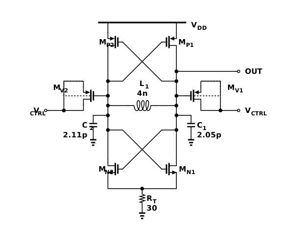
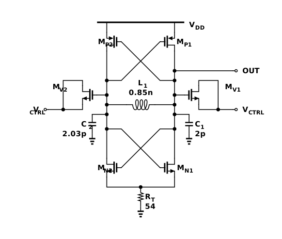
Baseline structure LC VCO: complementary cross-coupled pairs on a resistor tail (no tail transistor), MOS varactors

OpenSKY130 · ngspice

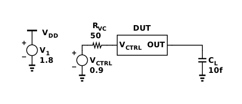
Testbench (SKY130): 1.8 V supply, 0.9 V through 50 Ω on VCTRL, 10 fF load on OUT; every inductor gets Q = 10Testbench.tran + LPTV noise · PVTSKY130Baseline: LC VCO: complementary cross-coupled pairs on a resistor tail (no tail transistor), MOS varactorsBaseline

Baseline −185.5 dB

Frequency2.1 GHz
Power5.15 mW
L(1 MHz)−126.2 dBc/Hz
White-noise FoM−185.6 dB
1/f3 corner35.5 kHz
Tuning, swing1 % over ±0.1 V, 1.51 V

Gates for any design Starts at every PVT corner; fosc 1.9 GHz to 2.3 GHz; monotonic tuning ≥ 1 % over ±0.1 V; swing ≥ 1.2 V

Previous baseline current-starved ring oscillator: −148.0 dB, score −3.75

ClosedGF22 22FDX+ · Spectre

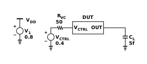
Testbench (GF22 22FDX+): 0.8 V supply, 0.4 V through 50 Ω on VCTRL, 5 fF load on OUT; PDK spiral inductorsTestbenchPSS + pnoise · PVTGF22 22FDX+Baseline: LC VCO: complementary cross-coupled pairs on a resistor tail (no tail transistor), MOS varactorsBaseline

Baseline −185.3 dB

Frequency5.11 GHz
Power1.64 mW
L(1 MHz)−113.2 dBc/Hz
White-noise FoM−186.4 dB
1/f3 corner300 kHz
Tuning, swing1 % over ±0.1 V, 586 mV

Gates for any design Starts at every PVT corner; fosc 4.5 GHz to 5.5 GHz; monotonic tuning ≥ 1 % over ±0.1 V; swing ≥ 500 mV

Previous baseline current-starved ring oscillator: −155.1 dB, score −3.02

Q7VCO architecture that minimises flicker (1/f3) phase noise

Minimise the 1/f3 phase-noise corner

Baseline structure LC VCO: complementary cross-coupled pairs on a resistor tail (no tail transistor), MOS varactors

OpenSKY130 · ngspice

Testbench (SKY130): 1.8 V supply, 0.9 V through 50 Ω on VCTRL, 10 fF load on OUT; every inductor gets Q = 10Testbench.tran + LPTV noise · PVTSKY130Baseline: LC VCO: complementary cross-coupled pairs on a resistor tail (no tail transistor), MOS varactorsBaseline

Baseline 35.5 kHz

Frequency2.1 GHz
Power5.15 mW
L(1 MHz)−126.2 dBc/Hz
White-noise FoM−185.6 dB
1/f3 corner35.5 kHz
Tuning, swing1 % over ±0.1 V, 1.51 V

Gates for any design Starts at every PVT corner; fosc 1.9 GHz to 2.3 GHz; monotonic tuning ≥ 1 % over ±0.1 V; swing ≥ 1.2 V; white-noise FoM ≤ −182.0 dB

Previous baseline current-starved ring oscillator: 7.87 MHz, score −2.35

ClosedGF22 22FDX+ · Spectre

Testbench (GF22 22FDX+): 0.8 V supply, 0.4 V through 50 Ω on VCTRL, 5 fF load on OUT; PDK spiral inductorsTestbenchPSS + pnoise · PVTGF22 22FDX+Baseline: LC VCO: complementary cross-coupled pairs on a resistor tail (no tail transistor), MOS varactorsBaseline

Baseline 300 kHz

Frequency5.11 GHz
Power1.64 mW
L(1 MHz)−113.2 dBc/Hz
White-noise FoM−186.4 dB
1/f3 corner300 kHz
Tuning, swing1 % over ±0.1 V, 586 mV

Gates for any design Starts at every PVT corner; fosc 4.5 GHz to 5.5 GHz; monotonic tuning ≥ 1 % over ±0.1 V; swing ≥ 500 mV; white-noise FoM ≤ −183.0 dB

Previous baseline current-starved ring oscillator: 9.79 MHz, score −1.51

Q8On-chip oscillator that minimises Δf/Trange

Minimise frequency drift from −40 to 125 °C, 13 points

Baseline structure RC relaxation oscillator: comparator with resistive hysteresis, both thresholds a fixed fraction of VDD, divider temperature-compensated by a high-TC share of the feedback resistor (high-poly in SKY130, n+ diffusion in GF22)

OpenSKY130 · ngspice

Testbench (SKY130): 1.8 V supply, 50 fF load on OUT; 13 temperatures from −40 to 125 °C, ±10 % supply, every cornerTestbench.tran · 13 temperatures · cornersSKY130Baseline: RC relaxation oscillator: comparator with resistive hysteresis, both thresholds a fixed fraction of VDD, divider temperature-compensated by a high-TC share of the feedback resistor (high-poly in SKY130, n+ diffusion in GF22)Baseline

Baseline 6.8 ppm/°C

Frequency at 27 °C2.14 MHz
Supply sensitivity5.1 %/V
Power13.4 µW
Swing1.78 V

Gates for any design 1 MHz to 10 MHz; P ≤ 100 µW; supply sensitivity ≤ 10 %/V; swing ≥ 900 mV; oscillates at every corner

Previous baseline three-stage RC ring: 210.0 ppm/°C, score −1.49

ClosedGF22 22FDX+ · Spectre

Testbench (GF22 22FDX+): 0.8 V supply, 20 fF load on OUT; 13 temperatures from −40 to 125 °C, ±10 % supply, every cornerTestbench.tran · 13 temperatures · cornersGF22 22FDX+Baseline: RC relaxation oscillator: comparator with resistive hysteresis, both thresholds a fixed fraction of VDD, divider temperature-compensated by a high-TC share of the feedback resistor (high-poly in SKY130, n+ diffusion in GF22)Baseline

Baseline 12.8 ppm/°C

Frequency at 27 °C2.66 MHz
Supply sensitivity8.5 %/V
Power15.5 µW
Swing795 mV

Gates for any design 1 MHz to 10 MHz; P ≤ 50 µW; supply sensitivity ≤ 20 %/V; swing ≥ 400 mV; oscillates at every corner

Previous baseline three-stage RC ring: 337.0 ppm/°C, score −1.42

Model resultspreliminary · Qwen3.5-9B

Scores are against the current baselines: 0 is the baseline, positive is better. So far no model has beaten a baseline. Runs of two larger models were stopped before they finished; their results will be added here.

With simulator feedback

The model writes the DUT netlist, gets every measurement and gate back and revises it. Best of 6 rounds over two runs; a netlist that breaks the device rules is sent back before simulation.

Open · SKY130Closed · GF22
Q1 Amplifier, max f_u/Pno score · fails: gain at PVT cornersno score · fails: gain at PVT corners, phase margin at PVT corners, f_u at PVT corners
Q2 Amplifier, min v²Pno score · fails: gain at PVT corners, phase margin at PVT corners, f_u at PVT cornersno score · fails: gain at PVT corners, phase margin at PVT corners, f_u at PVT corners
Q3 Comparator, min T·E−0.00 same as the baselineno score · fails: no decision at a PVT corner, offset, kickback
Q4 Comparator, min v²E−0.13 passes every gateno score · fails: no decision at a PVT corner, too slow
Q5 Phase detector, min t²P−0.08 passes every gateno score · circuit does not work
Q6 VCO, min FoMno score · fails: frequency, tuning not monotonic, tuning range, swing, no start-up at a PVT cornerno score · fails: tuning range
Q7 VCO, min 1/f³ cornerno score · circuit does not work−0.08 passes every gate
Q8 Oscillator, min Δf/Tno score · fails: frequency, power, supply sensitivityno score · fails: frequency, power, supply sensitivity, swing, stops at a process corner

As an agent in a terminal

Harbor task per question (Terminal-Bench Science layout) with the terminus-2 agent: a shell in a container with ngspice, the SKY130 models and the measurement code; 2 hours and 100 steps per task; the instruction asks for a better topology. Open version. A final netlist that is not allowed or does not simulate scores −1.

Qwen3.5-9BTopology vs baseline
Q1 Amplifier, max f_u/P−1 · final netlist not allowed–
Q2 Amplifier, min v²P−1 · final circuit does not simulatesame
Q3 Comparator, min T·Estopped–
Q4 Comparator, min v²E−1 · final circuit does not simulatenew
Q5 Phase detector, min t²Pstopped–
Q6 VCO, min FoMstopped–
Q7 VCO, min 1/f³ cornerstopped–
Q8 Oscillator, min Δf/Tstopped–

Open questionsno testbench yet

  1. Q9ADC architecture that minimises the Schreier FoM

    FoMS = SNDR + 10 log(BW/P)

  2. Q10ADC architecture that minimises the Walden FoM

    FoMW = P/(2ENOB·fs)

  3. Q11A PLL FoM that properly normalises fIN

    The jitter–power FoM 10 log(σt2P/1 mW) leaves out the reference frequency.

  4. Q12A DC-DC converter FoM that properly normalises the conversion ratio

    Efficiency alone does not account for Vout/Vin.

  5. Q13The system equation for LC-VCO noise with the transistor V–I model

    Phase noise of the LC VCO derived from the device's actual V–I characteristic, not an ideal −gm.

  6. Q14The proper FoM for a delay line as a function of delay and noise

    Delay, jitter and power in one figure of merit.

Design challengesDC, AC and noise only

Runnable questions, open version. SKY130 with ngspice. ngspice has no pss/pnoise, so noise of clocked circuits and oscillators is computed from the transient by linear periodically time-varying analysis; it matches kT/C to 0.3 %, LC-oscillator phase-noise theory to 0.2 dB, a transient-noise Monte Carlo of the StrongARM to 5 % and the ISF prediction of flicker upconversion to 0.6 %. SKY130 has no inductor model, so the VCO bench gives every inductor Q = 10 at 2.1 GHz. The oscillator bench steps at most 0.2 ns, which places each switching instant to a few ppm of the period.

Runnable questions, closed version. GF22 22FDX+ with Cadence Spectre 24.1 (0.8 V devices, PDK spiral inductors, MOM capacitors, poly resistors), using Spectre's own analyses: ac and noise; transient and transient noise; PSS and pnoise. VCO phase noise is the PM part of pnoise; on a ring oscillator the period jitter it implies (0.36 ps) matches Spectre transient noise (0.35 ps).

Both versions. Figures of merit are measured at tt, 27 °C; gates hold at 5 corners × 3 temperatures, and the comparator offset comes from 100 mismatch Monte Carlo samples. Score is log10 of the improvement over that version's baseline (dB figures of merit: difference/10). Each baseline is the best structure we know and could make work for its question. Under it is the previous baseline, the textbook circuit we started from, with its score against the new one. The DUT gets only the ports shown.

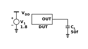
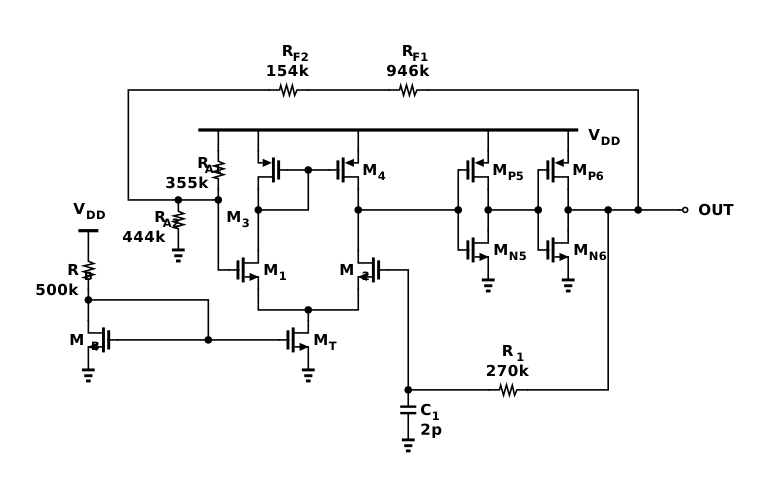
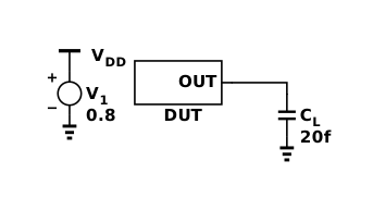
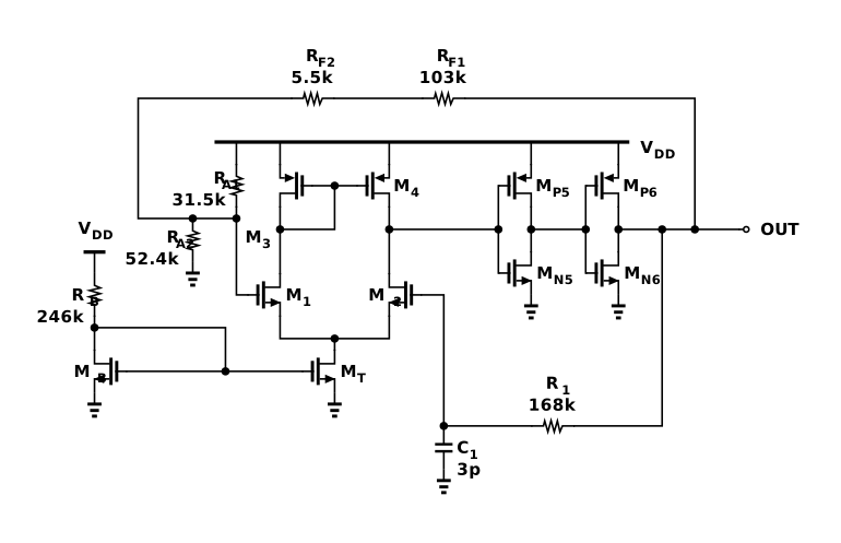
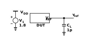
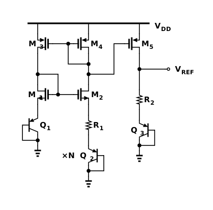
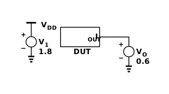
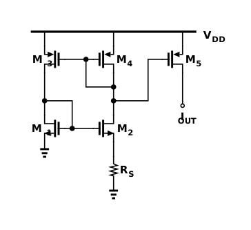
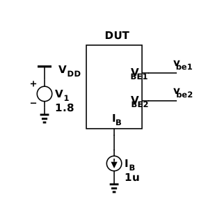
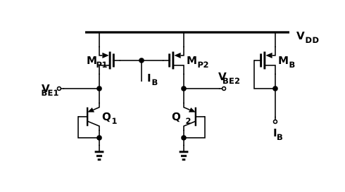
Design challenges. The testbench (supply, sources, loads and bias currents) is fixed; a submission replaces only the DUT block, built from PDK devices. Gates must pass at 5 corners × 3 temperatures × 3 supplies plus 200 Monte Carlo samples, with saturation margin on every transistor and no right-half-plane poles. Score is log10 of the improvement over the baseline design, which scores 0. All schematics are drawn with Analog Canvas and checked against reference netlists.